第一章 单元测试
1、单选题:
Which of the following is not a commonly used semiconductor material’? ( )
选项:
A:silicon
B:germanium
C:lead
D:carbon
答案: 【lead】
2、单选题:
The characteristic of an ideal diode are those of a switch that can conduct current( ) .
选项:
A:in both directions but in only one direction at a time
B:in one direction only
C:depends on the circuit it is used in
D:in both directions
答案: 【in one direction only】
3、单选题:
When a diode is doped with either a pentavalent or a trivalent impurity its resistance will ( ) .
选项:
A:increase
B:decrease
C:make the resistance stable against variation due to temperature
答案: 【decrease】
4、单选题:
The piecewise linear model, equivalent circuit of the diode consists of ( ).
选项:
A:a battery, a small resistor, and the ideal diode
B:a junction capacitor, a battery, a small resistor, and the ideal diode
C:the ideal diode
D:a battery and the ideal diode
答案: 【a battery, a small resistor, and the ideal diode】
5、单选题:
When a p-n junction is reverse-biased, its junction resistance is ( ).
选项:
A:determined by the components that are external to the device
B:low
C:high
D:constantly changing
答案: 【high】
第二章 单元测试
1、单选题:
What is the value of the voltage dropped across forward-biased silicon diodes that are connected in parallel with each other? ( ).
选项:
A:0.7 V
B:0.35 V
C:11.3 V
D:1.4 V
答案: 【0.7 V】
2、单选题:
The resistor voltage and resistor current in this circuit are ( ).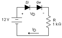
选项:
A:2 V, 11 mA
B:10 V, 5 mA
C:11 V, 11 mA
D:11 V, 2 mA
答案: 【11 V, 11 mA】
3、单选题:
Which of the following circuits is used to eliminate a portion of a signal? ( ).
选项:
A:Voltage divider
B:Clipper
C:Voltage multiplier
D:Damper
答案: 【Clipper】
4、单选题:
The circuit shown here is a ( ). 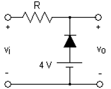
选项:
A:parallel clipper
B:series clipper
C:series clamper
D:shunt clamper
答案: 【parallel clipper】
5、单选题:
The Zener diode must be operated such that ( ).
选项:
A:the applied voltage is greater than 
B: is less than the specified
C:
D:All of these
答案: 【All of these】
第三章 单元测试
1、单选题:
In the active region, the base-emitter junction ( ).
选项:
A:and the base-collector junctions are both forward-biased
B:is reverse-biased while the base-collector junction is forward-biased
C:is forward-biased while the base-collector junction is reversed-biased
D:and the base-collector junctions are both reverse-biased
答案:
2、单选题:
A BJT has measured dc current values of  = 0.1 mA and
  = 8.0 mA. When IB is varied by 100 μA, IC changes by 10 mA. What is the value of the βac for this device?( ).
选项:
A:80
B:10
C:800
D:100
答案:
3、单选题:
When a BJT is operating in the active region, the voltage drop from the base to the emitter  is approximately equal to the ( )。
选项:
A:emitter voltage
B:base current times the base resistor
C:base bias voltage
D:diode drop (about 0.7 V)
答案:
4、单选题:
BJTs are commonly used as ( ).
选项:
A:the primary components in rectifiers
B:series damper circuits
C:the primary components in amplifiers
答案:
5、单选题:
The condition where increase in bias current will not cause further increases in collector current is called ( ).
选项:
A:saturation
B:active operation
C:cutoff
答案:
第四章 单元测试
1、单选题:
When a BJT is biased in the cutoff region the collector-to-emitter voltage is typically equal to ( ).
选项:
A:the collector supply voltage
B:the emitter voltage
C:the collector current times the collector resistor
D:0.03 V
答案:
2、单选题:
Calculate the collector-emitter voltage for this emitter-stabilized circuit.( ) 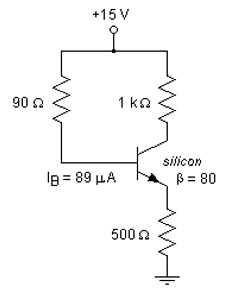
选项:
A:14.24 V
B:4.32 V
C:10.68 V
D:0.1335 V
答案:
3、单选题:
The difference between the resulting equations for a network in which an npn transistor has been replaced by a pnp transistor is ( ).
选项:
A:the value of β
B:the values of the resistors
C:the sign associates with the particular quantities
答案:
4、单选题:
The term quiescent means ( ).
选项:
A:inactive
B:at rest
C:active
D:midpoint-biased
答案:
5、单选题:
Voltage-divider bias stability is ( ).
选项:
A:dependent on alpha
B:dependent of beta
C:independent of beta
D:dependent on the collector resistor
答案:
第五章 单元测试
1、单选题:
Given this configuration, determine the input impedance if VS = 40 mV, Rsense = 0.5 kΩ, and the input current is 20 μA.( )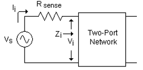
选项:
A:582 kΩ
B:1.5 MΩ
C:5.822 MΩ
D:1,500 Ω
答案:
2、单选题:
The  transistor model replaces the ( ) with the junction diode’s ac resistance.
选项:
A:collector-emitter junction
B:collector-base junction
C:emitter—base junction
答案:
3、单选题:
Calculate the voltage gain for this circuit. ( )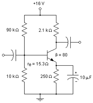
选项:
A:-8.4
B:-16.34
C: -7.91
D:-137.25
答案:
4、单选题:
A transistor amplifier has an input signal applied to its emitter terminal and an output signal taken from its collector terminal. The amplifier is a(n) ( ).
选项:
A:emitter follower
B:common-emitter amplifier
C:common-base amplifier
D:common-collector amplifier
答案:
5、单选题:
The voltage gain of a very well-designed common collector amplifier configuration, using a pnp transistor, is ( ).
选项:
A:in the range -0.95 to -0.99
B:about -0.9
C:in the range 0.95 to 0.99
D:about 0.9
答案:
第六章 单元测试
1、单选题:
Shockley’s equation defines the ( ) of the FET and are unaffected by the network in which the device is employed.
选项:
A:input/output characteristics
B:drain characteristics
C:transfer characteristics
D: characteristics
答案:
2、单选题:
For an n-channel depletion MOSFET,  = 8 mA and
  = -6 V. If
  = 0.8 V, what is the value of the drain current,
  ? ( )
? ( )
选项:
A:8 mA
B:6 mA
C:10.28 mA
D:10.25 μA
答案:
3、单选题:
The region of the JFET drain curve that lies between pinch-off and breakdown is called ( ).
选项:
A:the saturation region
B:the constant-voltage region
C:the ohmic region
答案:
4、多选题:
In the family of FETs, you can expect to find ( ).
选项:
A:an n-channel type
B:a p-channel type
C:unipolar structure
答案:
5、多选题:
FETs usually ( ).
选项:
A:are less sensitive to temperature change than BJTs
B:
are smaller in construction than BJTs
C:have a higher input impudence than BJTs
答案:
第七章 单元测试
1、单选题:
This graphical solution represents ( ).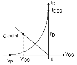
选项:
A:self bias for an n-channel JFET
B:fixed bias for an n-channel JFET
C:voltage-divider bias for an n-channel JFET
答案:
2、单选题:
Generally, it is good design practice for linear amplifiers to have operating points that close to ( ).
选项:
A:are close to saturation level
B:the midpoint of the load line
C:the cut-off region
答案:
3、单选题:
Which of the following biasing circuits can be used with E-MOSFETs? ( )
选项:
A:current-source bias
B:drain-feedback bias
C:zero bias
D:self bias
答案:
4、单选题:
The primary difference between JFETs and depletion-type MOSFETs is ( ).
选项:
A:depletion-type MOSFETs can have only positive of 
B:JFETs can have only positive values of 
C:depletion-type MOSFETs can have positive values of  and levels of
  that exceed
D:JFETs can have positive values of  and levels of drain current that exceed
答案:
5、多选题:
A JFET can be biased in several different ways. The common method(s) of biasing an n-channel JFET is(are) ( ).
选项:
A:fixed-bias configuration
B:voltage-divider bias configuration
C:self-bias configuration
答案:
第八章 单元测试
1、单选题:
The FET version of the BJT’s common-emitter configuration is the ( ) circuit.
选项:
A:common-source
B:common-current
C:common-gate
D:common-drain
答案:
2、单选题:
Calculate the input impedance for this FET amplifier. ( )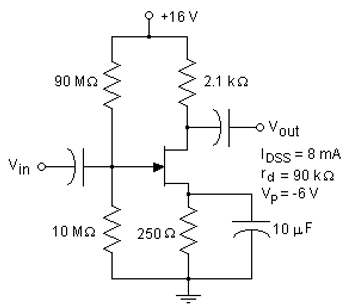
选项:
A: = would depend on the drain current
B:
C:
D:
答案:
3、单选题:
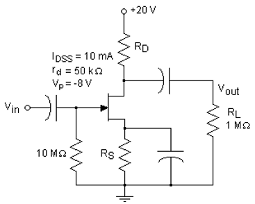
Design this circuit for a voltage gain of 10. You have to calculate the value of resistor  and
and  . It is desired that the transistor operate with a relatively high value of
  . For this device, a high value of
  is defined as
  . ( )
. ( )
选项:
A:
B:
C:
D:
答案:
4、单选题:
The ( ) amplifier has high input impedance, low output impedance, and low voltage gain.
选项:
A:common-source
B:common-drain
C:common-gate
答案:
5、单选题:
The ( ) FET amplifier has low input impedance, high output impedance, and high voltage gain.
选项:
A:common-source
B:common-drain
C:common-gate
答案:
第九章 单元测试
1、单选题:
Calculate the low frequency break point due to the capacitor  for this BJT amplifier. ( )
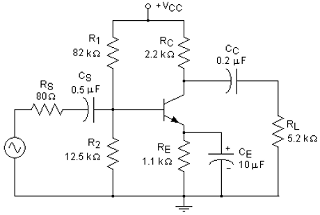
选项:
A:
B:
C:
D:
答案:
2、单选题:
If several identical stages of amplifiers, each having the exact same upper and lower cutoff frequencies, are connected in cascade, then the bandwidth of the resulting amplifier will ( ).
选项:
A:remain unchanged
B:decrease
C:be equal to the sum of all the individual bandwidths
D:increase
答案:
3、单选题:
A 3-dB drop in β occurs at ( ).
选项:
A:
B:
C:
D:
答案:
4、单选题:
Negative dB values represent ( ).
选项:
A:power values that do not change
B:power losses
C:power gain
答案:
5、单选题:
An amplifier has a midband power gain of 24,500. What is the value of the power gain in dB for the circuit? ( )
选项:
A:43.9 dB
B:4.39 dB
C:87.78 dB
答案:
第十章 单元测试
1、单选题:
Under difference-mode operation, the difference-mode voltage gain for this circuit is ( ).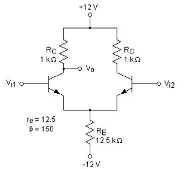
选项:
A:0.0397
B:80
C:40
D:0.08
答案:
2、单选题:
The operational amplifier will only slightly amplify signals ( ).
选项:
A:when the supply voltages are more then ±25 V
B:that are different on both the inputs
C:that are common on both the inputs
D:when the supply voltages are less then ±5 V
答案:
3、单选题:
The inverting and noninverting inputs to an op-amp are used to drive a(n) ( ) amplifier.
选项:
A:noninverting
B:inverting
C:open-loop
D:differential
答案:
4、单选题:
When a given op-amp has a common-mode input of 10 V, the output of the device is 10 V. When the device has a differential input of 2 mV, the output of the device is 10 V. What is the CMPR of the device? ( )
选项:
A:5000 : 1
B:5 : 1
C:5,000,000 : 1
D:1000 : 1
答案:
5、多选题:
The bandwidth of an amplifier is ( ).
选项:
A: the range of frequencies found using 
B:the range of frequencies between the lower and upper 3 dB frequencies
C:the range of frequencies over which gain remains relatively constant
答案:
第十一章 单元测试
1、单选题:
If the input voltage is 0.25 V and the output is -2.5 V, the value of must be ( ).
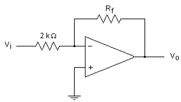
选项:
A:20.0 kΩ
B:16.0 kΩ
C:5.0 kΩ
D:40.0 kΩ
答案:
2、单选题:
The output voltage, VO, is given by ( ).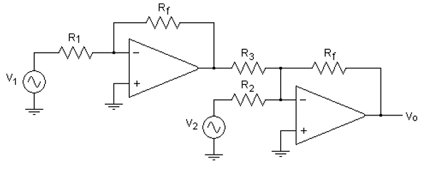
选项:
A:
B:
C:
答案:
3、单选题:
A summing integrator is an op-amp integrator that has ( ).
选项:
A:multiple feedback capacitors
B:multiple input resistors and feedback capacitors
C:multiple input resistors
答案:
4、单选题:
A second order low-pass filter has a high-end roll-off of ( ).
选项:
A:40 dB/decade
B:20 dB/octave
C:60 dB/octave
D:6 dB/decade
答案:
5、单选题:
An active filter that provides a constant output for input signals above  is called an ideal ( ).
选项:
A:bandpass filter
B:high-pass filter
C:low-pass filter
答案:
第十二章 单元测试
1、单选题:
A class B amplifier (not push-pull) ( ).
选项:
A:conducts through less than 180° of the input waveform
B:conducts through 180° of the input waveform
C:conducts between 180° and 360° degrees of the input waveform, depending on the amount of dc bias
D:conducts through 360° of the input waveform
答案:
2、单选题:
Crossover distortion in class B amplifiers is prevented by ( ).
选项:
A:biasing the transistors deeply into cutoff
B:biasing the transistors slightly above cutoff
C:using complementary-symmetry transistors
D:increasing the load resistance
答案:
3、单选题:
The maximum theoretical efficiency of an RC-coupled class A amplifier is ( ).
选项:
A:25%
B:99%
C:78.5%
D:50%
答案:
4、判断题:
Power amplifiers are typically used to drive low impedance loads.( )
选项:
A:错
B:对
答案:
5、判断题:
The power that an amplifier delivers to a load is equal to the difference between the power that the circuit draws from the power supply and the power that the circuit dissipates.( )
选项:
A:错
B:对
答案:
第十三章 单元测试
1、单选题:
The feedback circuit connection shown here is ( ).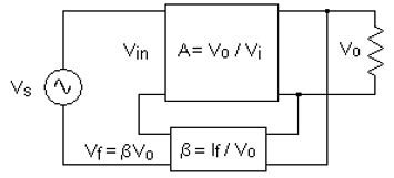
选项:
A:voltage series feedback
B:current series feedback
C:current shunt feedback
D:voltage shunt feedback
答案:
2、单选题:
Calculate the voltage gain for voltage series feedback when the amplifier gain is A = -2000 and F = -1/50. ( )
选项:
A:-1/50
B:50
C:-2000
D:-48.78
答案:
3、单选题:
Calculate the input impedance for voltage series feedback when the amplifier has  = 10 kΩ, amplifier gain is A = -2000, and F=
  . ( )
. ( )
选项:
A:input impedance with feedback 410 kΩ
B:input impedance with feedback 50 Ω
C:input impedance with feedback 244 Ω
D:input impedance with feedback 10 kΩ
答案:
4、单选题:
The output impedance of current-shunt feedback amplifier ( ) the output impedance of its op-amp.
选项:
A:is reduced by half when compared to
B:is decreased when compared to
C:has no effect on
D:is increased when compared to
答案:
5、单选题:
An amplifier has a gain-bandwidth product of 200 MHz. A feedback network is added that has a feedback factor (1 + βA) of 18.88. What is the gain-bandwidth product for the circuit with the added feedback network? ( )
选项:
A:10.59 MHz
B:200 MHz
C:18.88 MHz
答案:


评论0